
Research
① 12-to-1V Distributed Converter Array with One-Pin Current Balancing
CICC 2026 · 180nm BCD & 65nm CMOS
② 20MHz-1MHz Dual-Loop NonUniform-Multi-Inductor Hybrid Converter
ISSCC 2025 Highlight · 180nm BCD
③ Fast-Slow Two-Module High-Power-Density DC-DC Converter
CICC 2024 / JSSC 2025 · 180nm BCD
④ Multi-Path Inductor-First Inductor-on-Ground Hybrid Converter
CICC 2023 / JSSC 2024 · 180nm BCD
⑤ Symmetrical Double Step-Down Converter with Extended VCR
TCAS-I 2022 · 65nm CMOS
My research interests include power-management ICs (PMICs)—particularly high-voltage-conversion-ratio DC–DC converters and highly integrated on-chip and in-package voltage regulators (IVRs)—with an emphasis on high current density, high efficiency, fast transient response, and easy scalability.
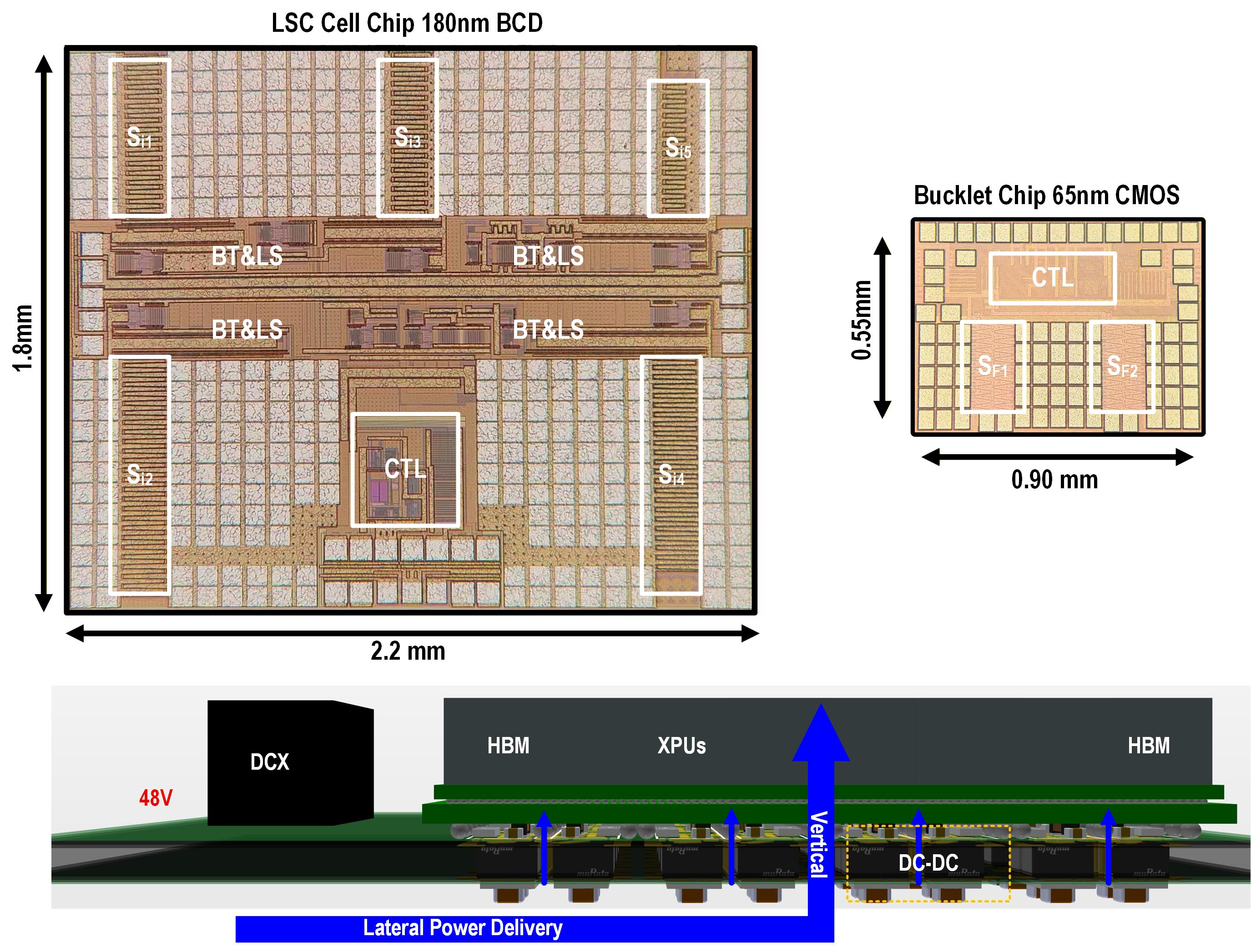
1) A Scalable Distributed 12-to-1V Fast-Slow Hybrid DC-DC Combo with Fast-Transient Bucklets and One-Pin Current Balancing
Challenge: As single-package current scales toward hundreds of amperes, centralized parallel control becomes a routing bottleneck with O(N) interconnect complexity, causing current imbalance and transient de-synchronization.
Approach: Distributed local feedback with a single shared one-pin bus for current self-balancing. Each unit performs autonomous local control; inter-module communication is reduced to O(1). The one-pin bus passively equalizes currents without high-bandwidth digital links.
Highlights:
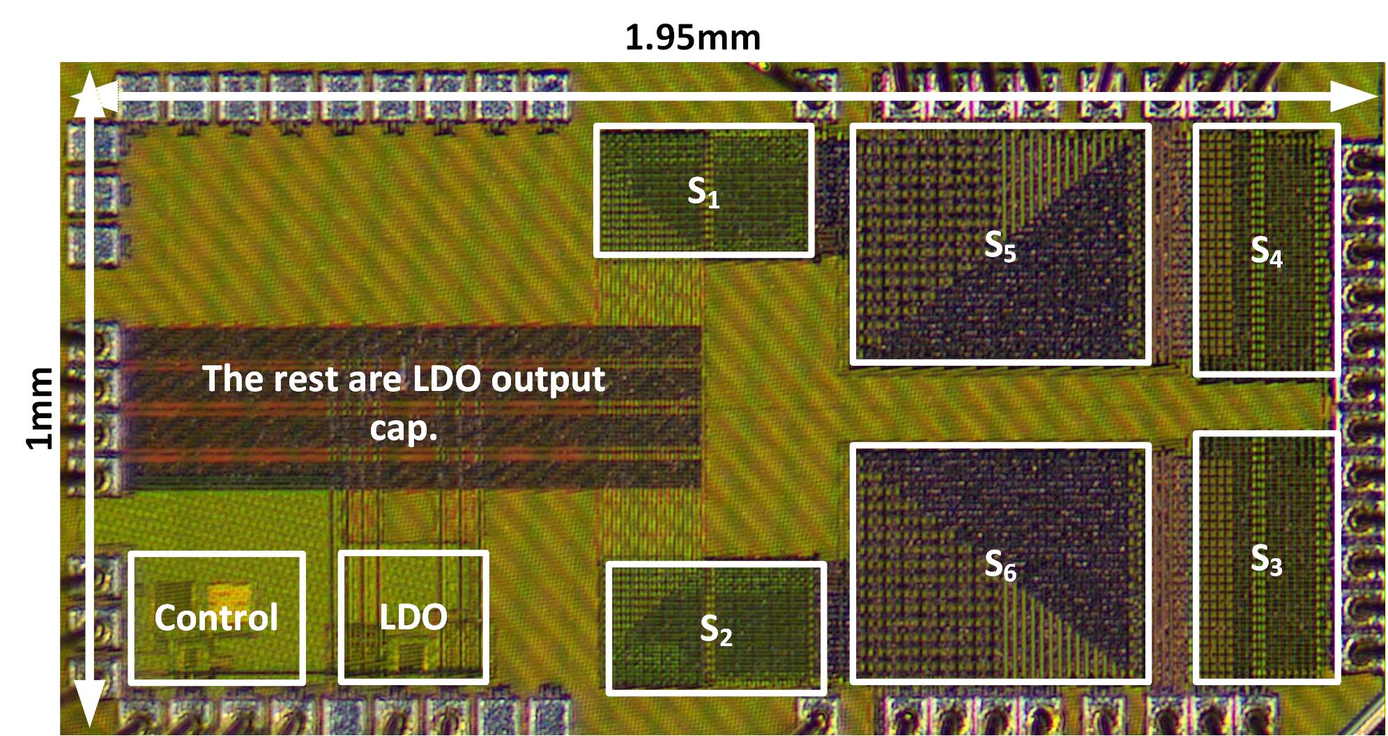
- 4-phase array: 12V to 1V, 22 A output; 89.1% peak efficiency; 1.46 A/mm² current density
- 6A / 20ns load step: ~55 mV undershoot, 2.2 µs recovery
- Directly applicable to Power Chiplet and vertical power delivery architectures
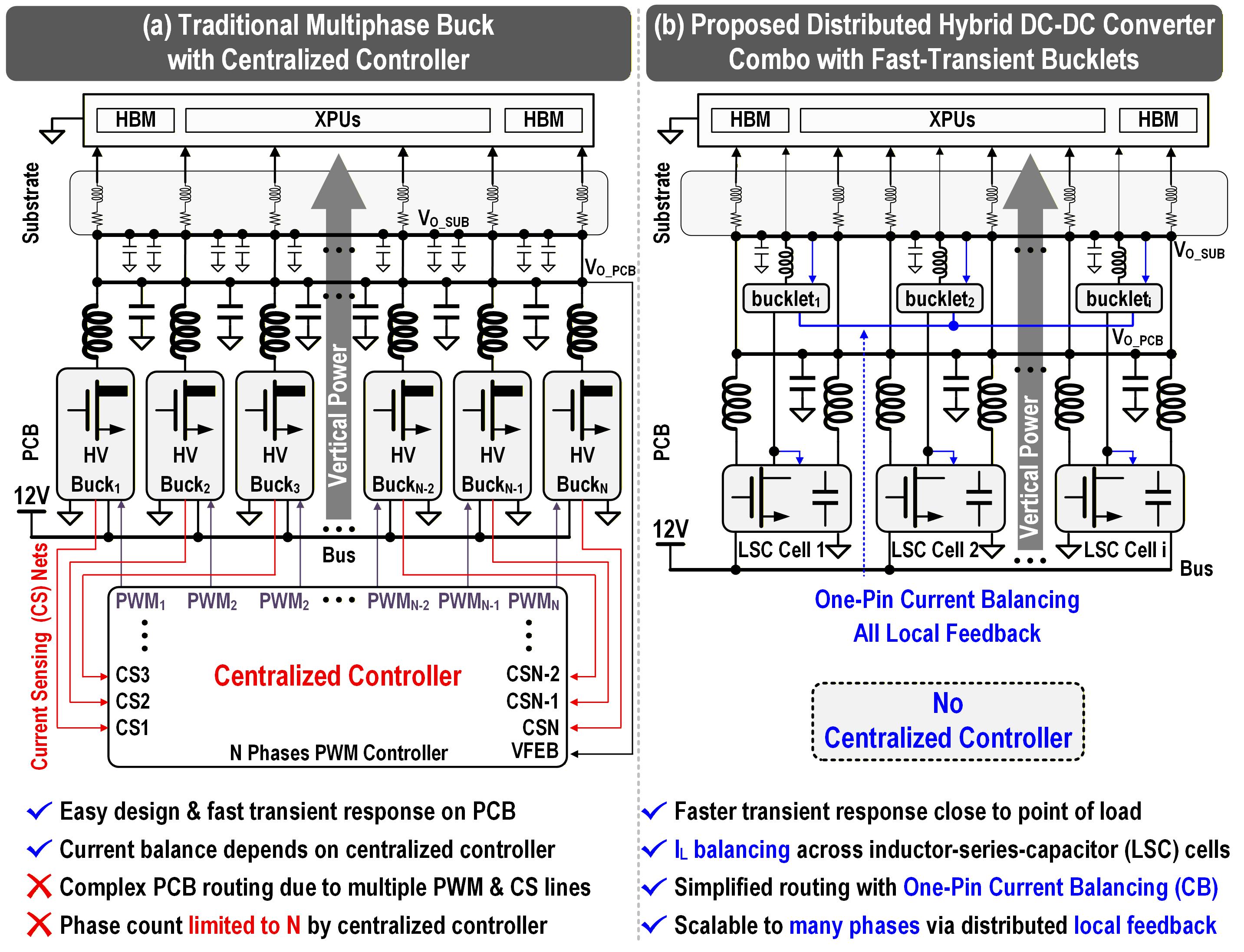
Accepted at CICC (2026)
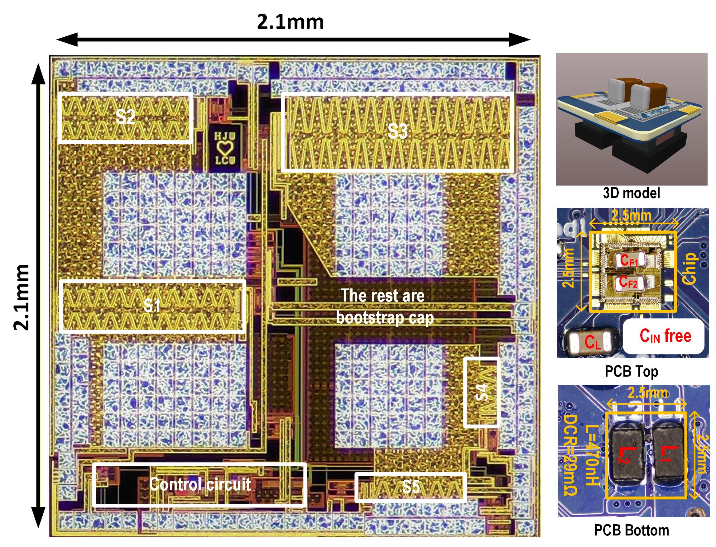
2) A 20MHz-1MHz Dual-Loop NonUniform-Multi-Inductor Hybrid DC-DC Converter with Specified Inductor Current Allocation and Fast Transient Response
Challenge: High-VCR bus-powered supplies face a fundamental tension: optimizing for efficiency limits bandwidth, and vice versa.
Approach: A fast-slow dual-module architecture on a single chip with dedicated dual-loop control: a slow module (~1 MHz) handles the high-VCR efficiency path; a fast module (~20 MHz) handles transient injection at high bandwidth. Bandwidth separation and coupled-loop stability are rigorously verified.
Highlights:
- Vout undershoot: 426 mV to 35 mV (12.2×); overshoot: 397 mV to 32 mV (12.4×)
- Dual-loop co-stability validated via small-signal modeling and silicon measurement
- Establishes a reusable “fast-slow split + dual-loop” design paradigm
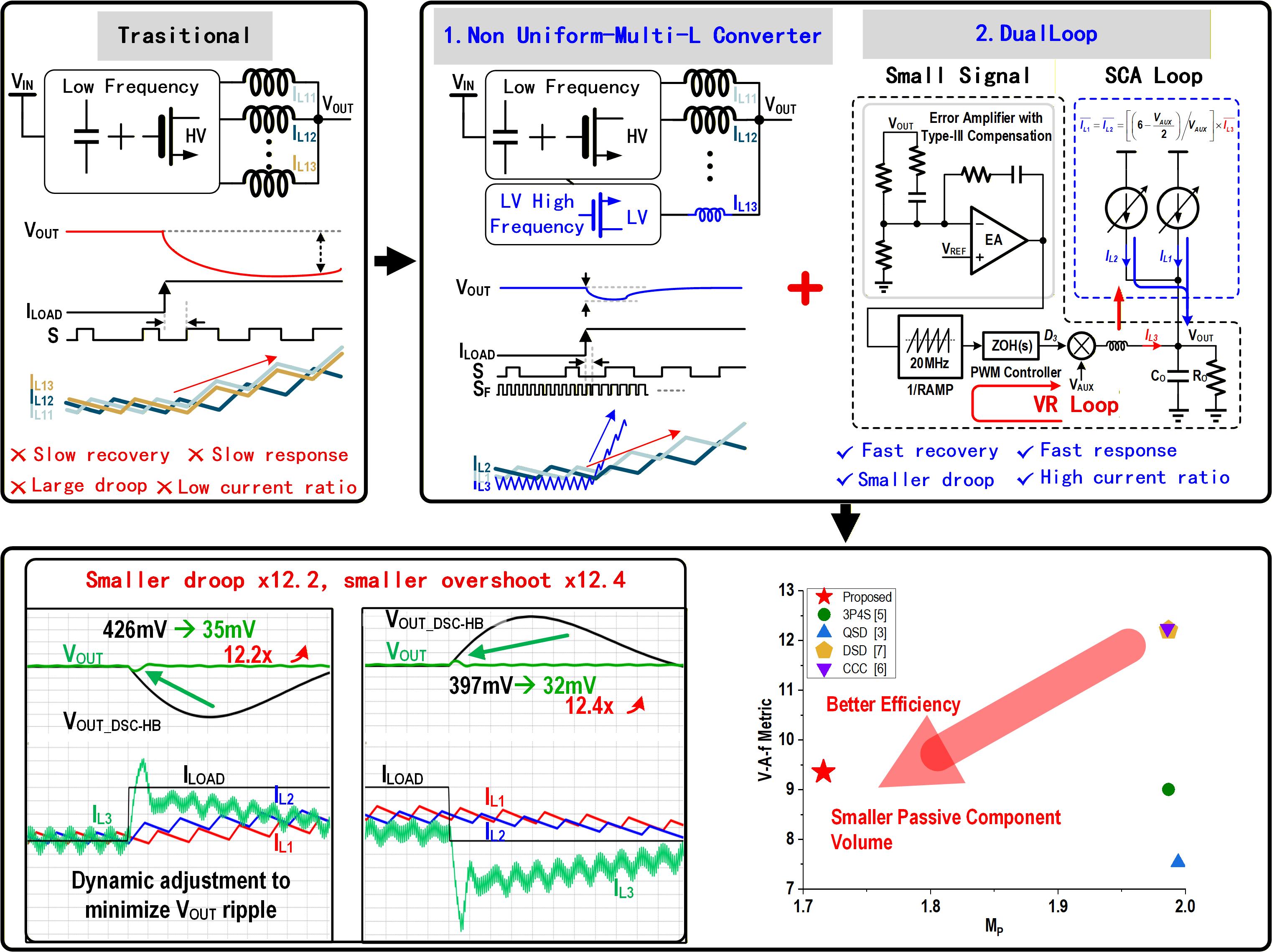
Published at ISSCC (2025, highlight paper)
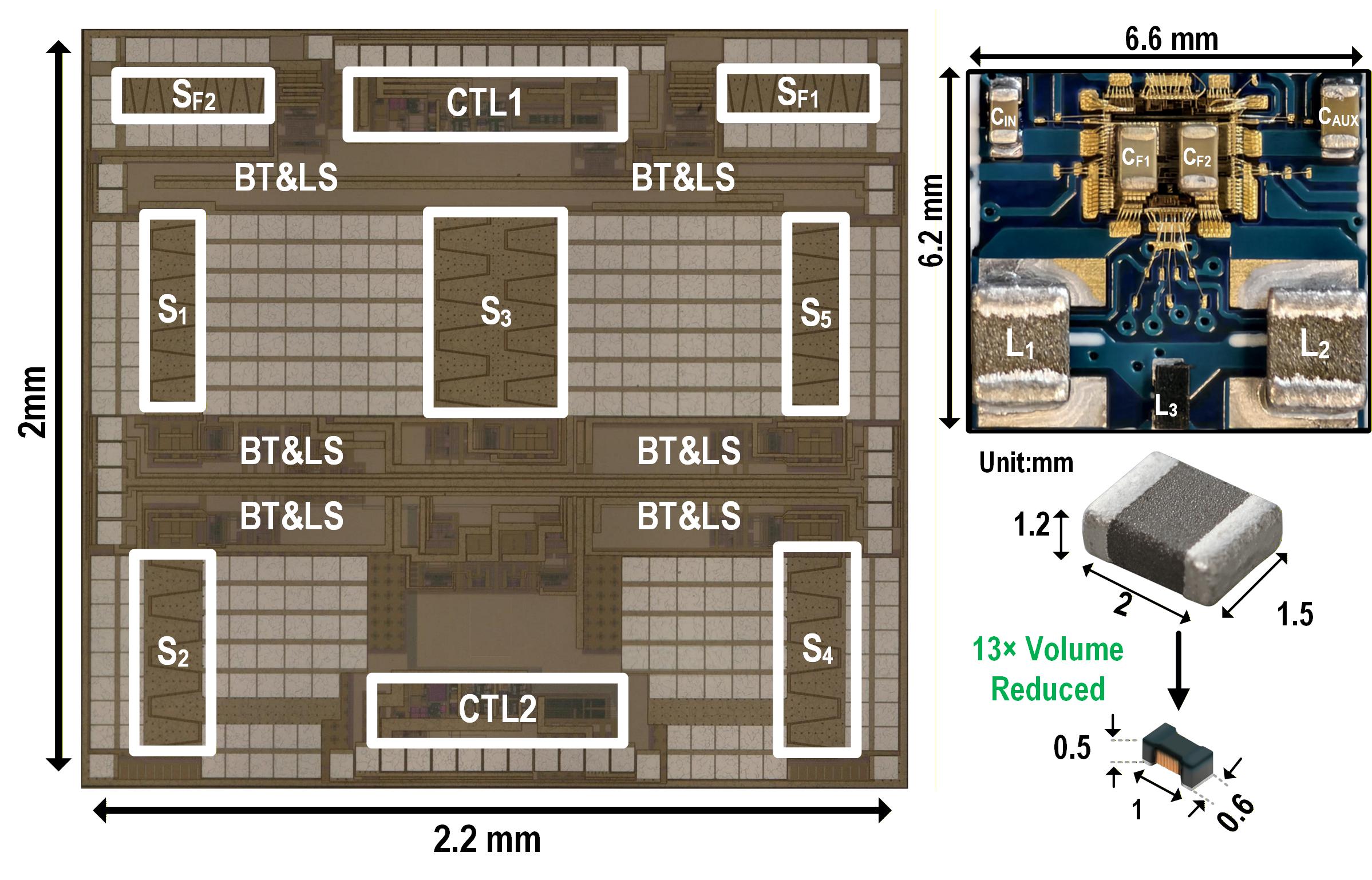
3) A Fast-Slow Two-Module High-Power-Density DC-DC Solution with Transient and Efficiency Improvements
Challenge: In 48V/12V bus-powered AI accelerator systems, load current slews at extremely high di/dt. Main stages optimized for steady-state efficiency suffer from large undershoot/overshoot and slow recovery.
Approach: I decouple the “efficiency” and “transient” tasks. The main HV power stage handles steady-state conversion; a small auxiliary module built with low-voltage core devices injects high di/dt current only during the critical transient window.
Highlights:
- Undershoot: 115 mV to 13 mV (8.8×); recovery: 80 µs to 2.5 µs (32×)
- Overshoot: 145 mV to 22 mV (6.6×); recovery: 35 µs to 3 µs (11.7×)
- Main stage efficiency unaffected; auxiliary module is plug-in compatible
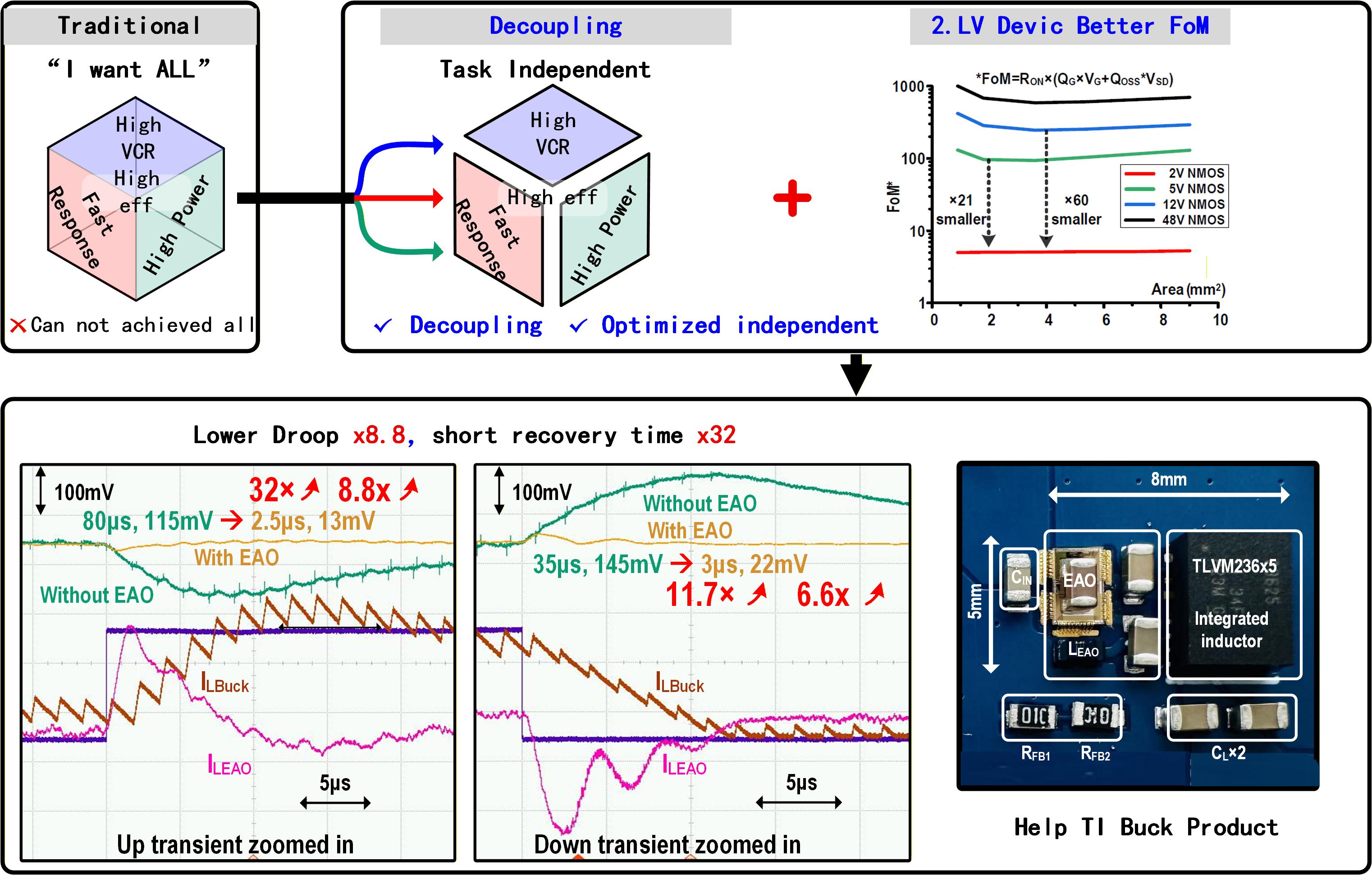
Published at CICC (2024); extended version in JSSC (2025)
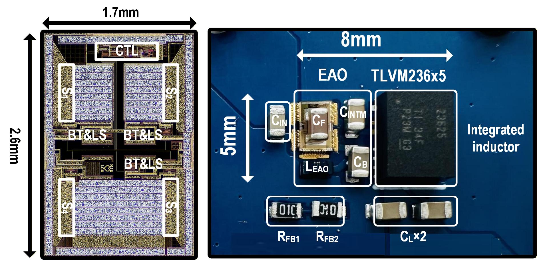
4) A Multi-Path Inductor-First Inductor-on-Ground Switched-Capacitor Hybrid DC-DC Converter
Challenge: Conventional hybrid converters place the inductor on the output (high-current) side, causing large DCR losses, high input current ripple, and dependence on bulky input capacitors.
Approach: I propose repositioning the inductor to the input or ground-referenced branch, so energy buffering moves upstream. This makes input current quasi-continuous, reduces input capacitor requirements, and lowers conduction loss at high-current nodes.
Highlights:
- Covers Vin = 3–5 V (Li-ion + 5V USB), Vout = 0.5–1.2 V, VCR up to 10:1
- 96.1% peak efficiency; 1.02 A/mm² current density (~2.3× over prior art)
- Reduced EMI due to continuous input current
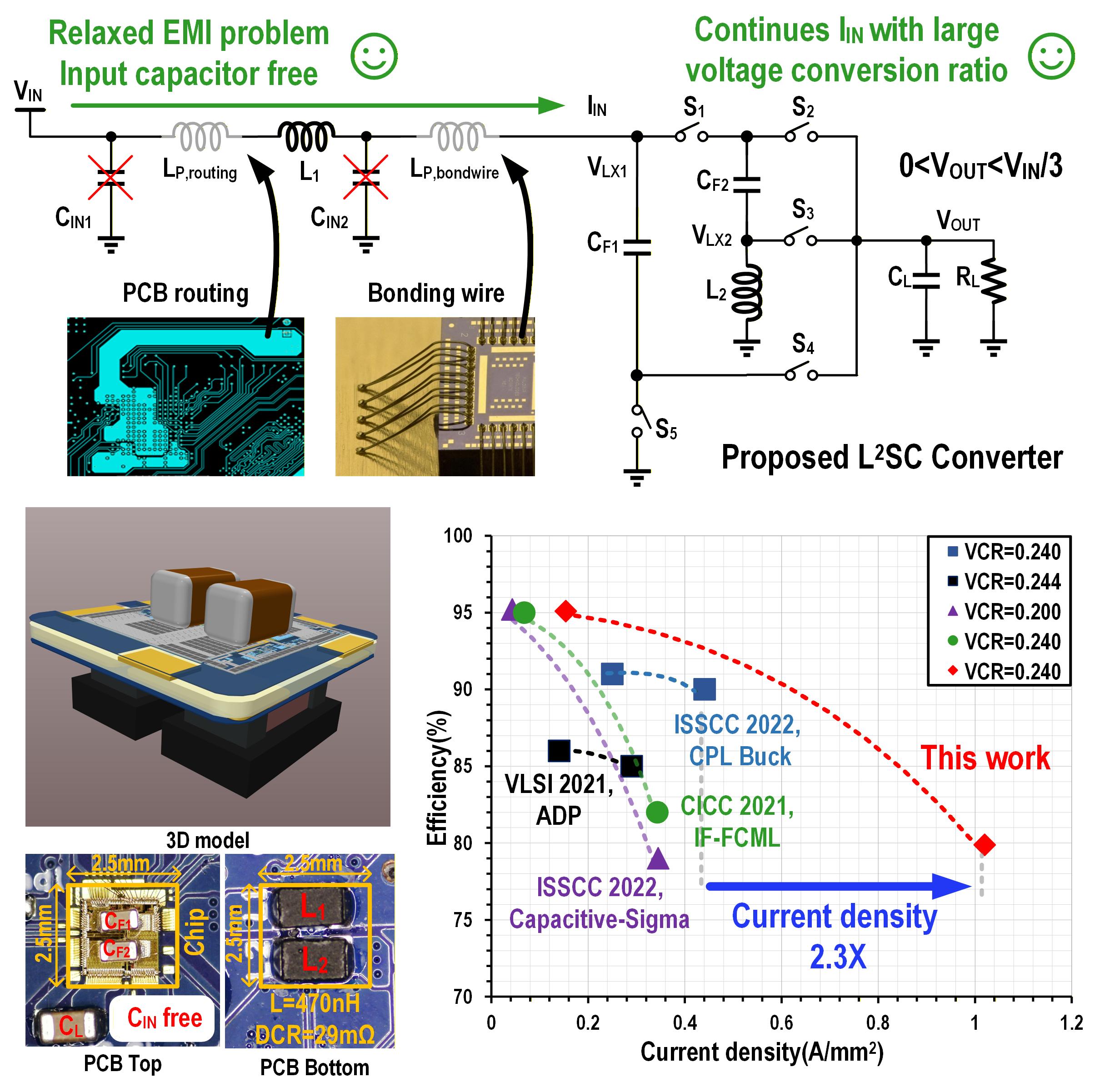
Published at CICC (2023); extended version in JSSC (2024)
5) A Symmetrical Double Step-Down Converter with Extended Voltage Conversion Ratio
Challenge: In battery-powered devices, the input voltage swings widely (2.7–4.2 V for Li-ion), while the processor core needs a tight low voltage (~0.5–0.8 V). Conventional Double Step-Down (DSD) hybrids are constrained to duty cycles D < 0.5, limiting their usable conversion ratio range.
Approach: By symmetrizing the DSD topology, I break the D < 0.5 constraint and extend the effective VCR range without adding switching stages. The symmetric structure equalizes inductor charging intervals, improving current density and reducing output ripple.
Highlights:
- Extends hybrid converter VCR range beyond the traditional D < 0.5 limit
- Improves efficiency across the full battery discharge range
- Validated in silicon; cited by groups at Dartmouth College, SCUT, and others
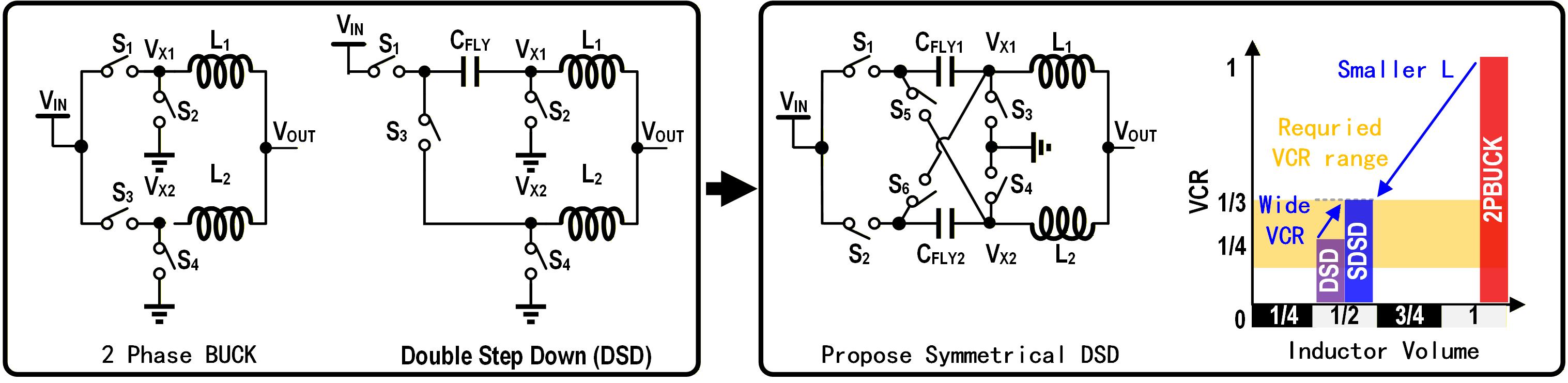
Published in TCAS-I (2022) · 65nm CMOS