Welcome to Junwei Huang’s Homepage
Hi! My name is Junwei Huang — a Postdoctoral Fellow at the Institute of Microelectronics, University of Macau, advised by Prof. Rui P. Martins, collaborating with Prof. Yan Lu (Tsinghua University). I’m currently a Visiting Postdoctoral Researcher in the Department of Electrical Engineering and Computer Sciences at the University of California, Berkeley, advised by Professor Robert Pilawa-Podgurski.
My research interests focus on integrated voltage regulators (IVRs) and power management ICs (PMICs) — particularly hybrid switched-capacitor/inductor DC-DC converters, high-conversion-ratio power delivery, fast transient response, vertical/chiplet power delivery, and scalable multi-module power systems.
You can find my CV here.
Research Highlights
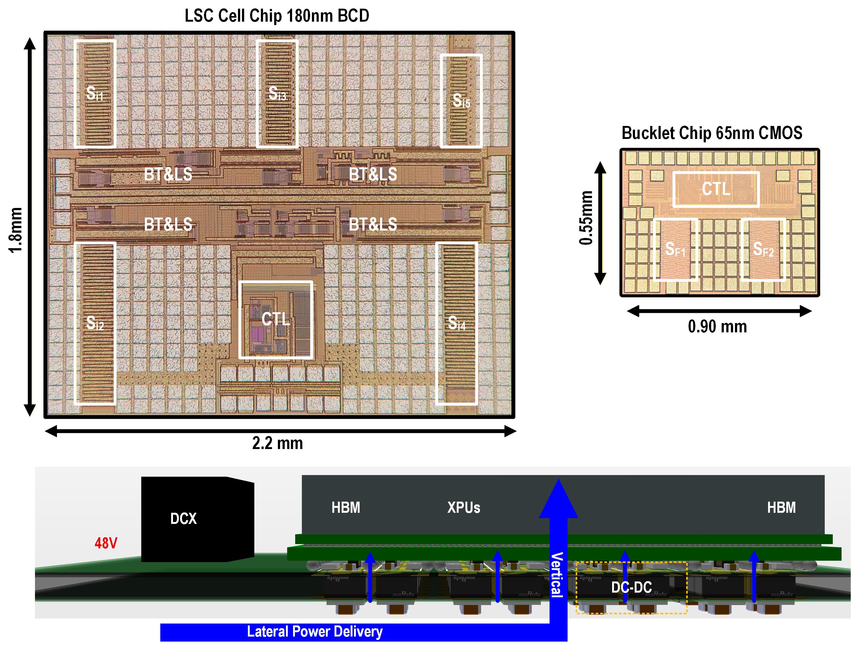
① 12-to-1V Distributed Converter Array with One-Pin Current Balancing
CICC 2026 · 180nm BCD & 65nm CMOS
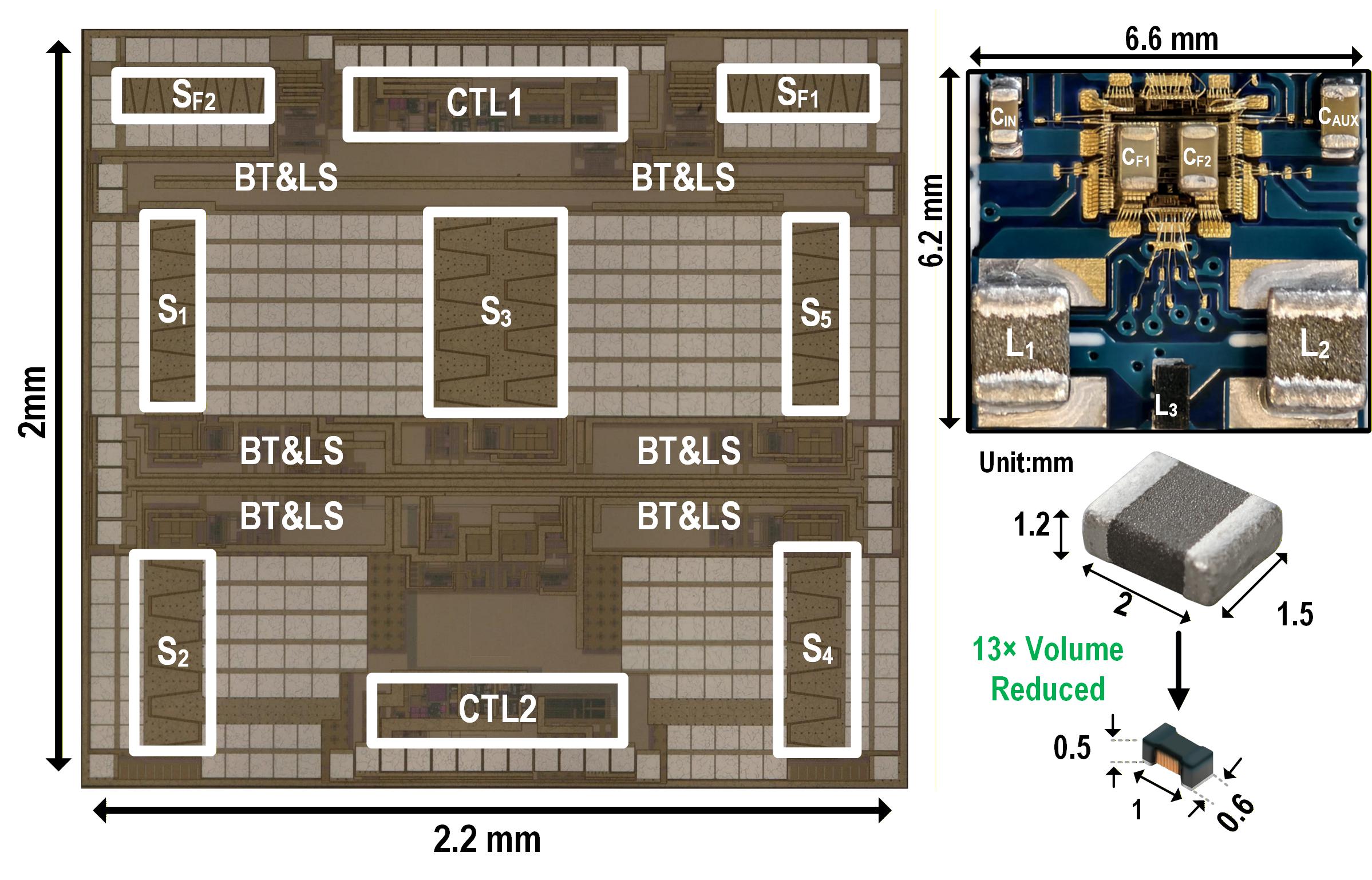
② 20MHz-1MHz Dual-Loop NonUniform-Multi-Inductor Hybrid Converter
ISSCC 2025 Highlight · 180nm BCD
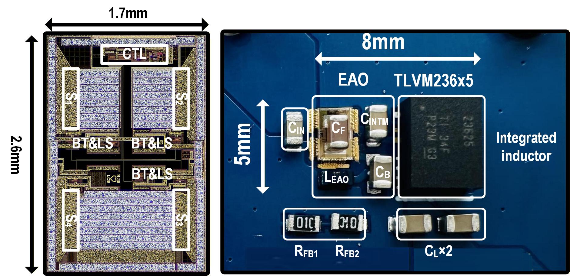
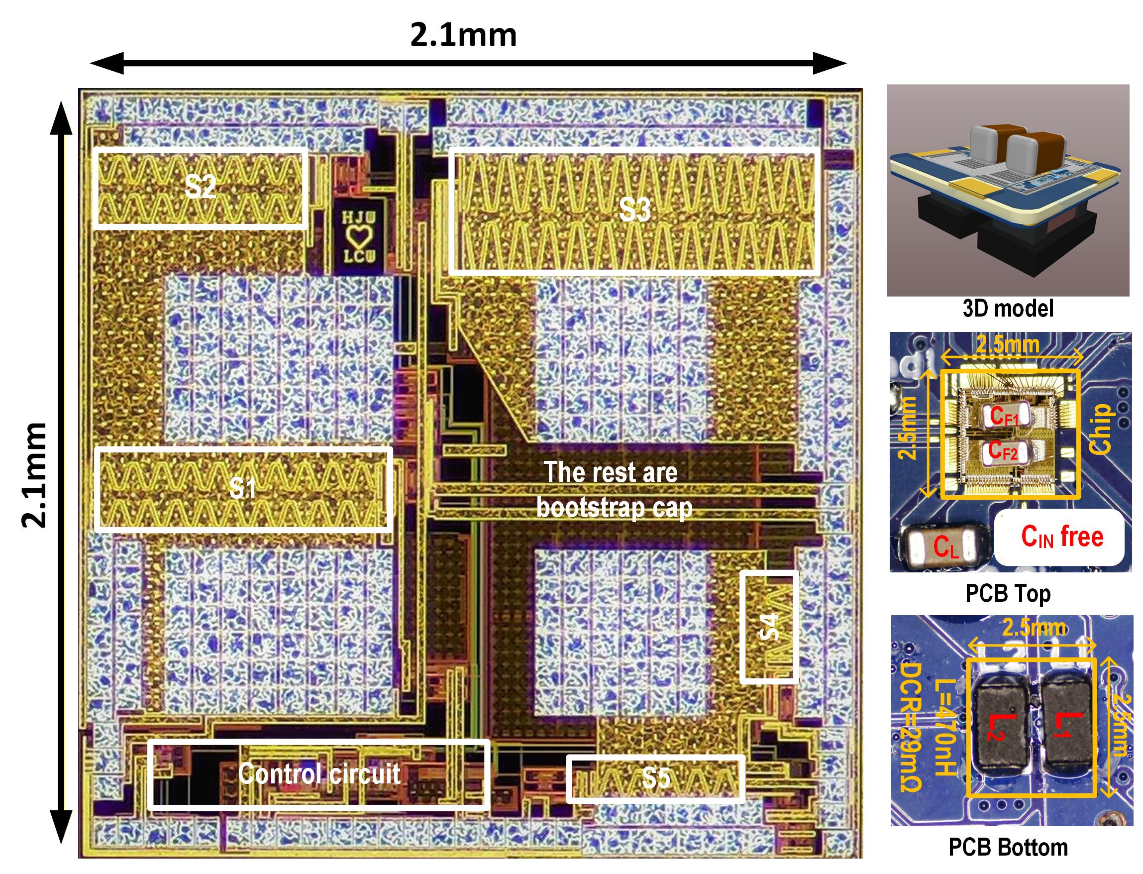
③ Fast-Slow Two-Module High-Power-Density DC-DC Converter
CICC 2024 / JSSC 2025 · 180nm BCD
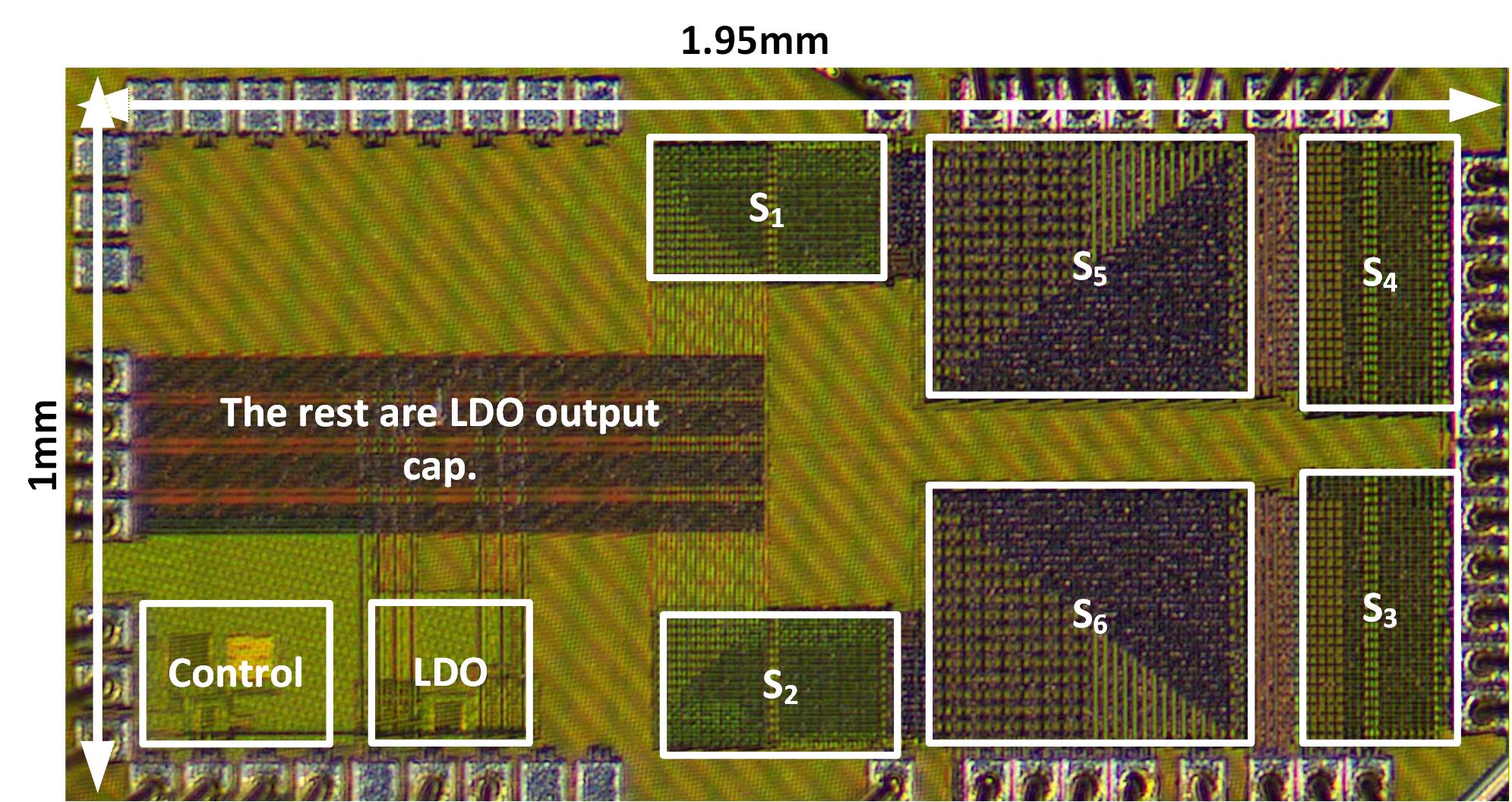
④ Multi-Path Inductor-First Inductor-on-Ground Hybrid Converter
CICC 2023 / JSSC 2024 · 180nm BCD
⑤ Symmetrical Double Step-Down Converter with Extended VCR
TCAS-I 2022 · 65nm CMOS
Education
Ph.D. in Electrical and Computer Engineering, University of Macau · 2018.08–2024.07
State Key Laboratory of Analog and Mixed-Signal VLSI (AMSV)
Advisors: Prof. Yan Lu and Prof. Chi-Seng LamB.Eng. in Microelectronics, University of Electronic Science and Technology of China (UESTC) · 2014–2018
Academic Appointments
Visiting Postdoctoral Researcher, Pilawa Power Electronics Research Group, EECS, University of California, Berkeley · 2025.09–present
Faculty Host: Prof. Robert Pilawa-PodgurskiPostdoctoral Fellow, Institute of Microelectronics (IME) & State Key Laboratory of Analog and Mixed-Signal VLSI, University of Macau · 2025.09–present
PIs: Prof. Rui P. Martins and Prof. Sai-Weng SinResearch Assistant, Institute of Microelectronics (IME), University of Macau · 2024.10–2025.09
PI: Prof. Rui P. MartinsVisiting Scholar, Department of Electronic Engineering, Tsinghua University · 2024.11–2025.05
Faculty Host: Prof. Yan Lu
Research Summary
University of California, Berkeley, EECS · 2025.09–present
Research focuses on the co-design of board-level power electronics and on-interposer high-voltage integrated voltage regulators (HV-IVR, >6 V input) for next-generation GPU/CPU power delivery, leveraging hybrid switched-capacitor/inductor converter topologies and scalable distributed converter arrays to achieve high aggregate current, high current density, and high power density.
University of Macau, State Key Lab of Analog and Mixed-Signal VLSI · 2018.08–2025.09
- Designed and taped out multiple hybrid SC/inductor DC-DC converters in 65 nm CMOS and 180 nm BCD processes, covering the full IC design cycle from topology innovation, circuit/layout implementation, to silicon measurement.
- Demonstrated state-of-the-art efficiency (96.1% at 4-to-1.2 V), current density (1.46 A/mm² at 12:1), and transient response (63 mV droop @ 3.5 A load step) across hybrid converters with conversion ratios from 4:1 to 12:1.
- Pioneered a scalable multi-module parallel architecture with one-pin decentralized current balancing, reducing interconnect complexity from O(N) to O(1) — directly applicable to IVR arrays and vertical power delivery.
- 25 publications: 1 ISSCC highlight paper (1st author), 3 CICC 1st-author, 2 JSSC 1st-author, 1 TCAS-I 1st-author. Total: 6 ISSCC + 6 JSSC contributions.
Technical Skills
- IC Design: Full-custom analog/mixed-signal IC design (schematic, layout, DRC/LVS, post-layout simulation, tape-out, lab measurement); switched-capacitor and hybrid DC-DC converter topologies; multi-loop control design; power stage optimization
- Process Technologies: 65 nm CMOS, 180 nm BCD (high-voltage NMOS/PMOS)
- EDA Tools: Cadence Virtuoso (Spectre, Layout XL), Ansys (HFSS/Maxwell), MATLAB/Simulink, Altium Designer (PCB)
- Lab Equipment: Oscilloscopes, spectrum analyzers, semiconductor parameter analyzers, probe stations; board-level power converter testing; multi-chip measurement and characterization
- Programming: SKILL (Cadence), Python, MATLAB, Verilog (digital control blocks)
Awards & Service
- Akrostar Technology Academic Prize for the academic year 2023/2024 (Top 3)
- Reviewer for IEEE TIE, IEEE OJIE, IEEE TCAS-I, IEEE TCAS-II, IEEE OJCAS
- Invited presenter at IEEE PES/PELS event at UC Berkeley